PCB, PCBA & FPC
Manufacturing Built Right
The global engineering portal of Shenzhen Lingxin Technology Co., Ltd. Fabrication from 1 to 44 layers, quick-turn prototypes from 24 hours, controlled impedance ±8% — plus free calculators that answer your stackup questions before you send a drawing.
Issued automatically once your email is verified · Minimum order $200 USD before discount · Valid 90 days · One coupon per member account, not combinable with other promotions.
Choose the line your project belongs to
Every enquiry starts in one of three places. Pick the one that matches your board, and we route it to the right process engineer — no general-purpose contact form.
PCB Manufacturing
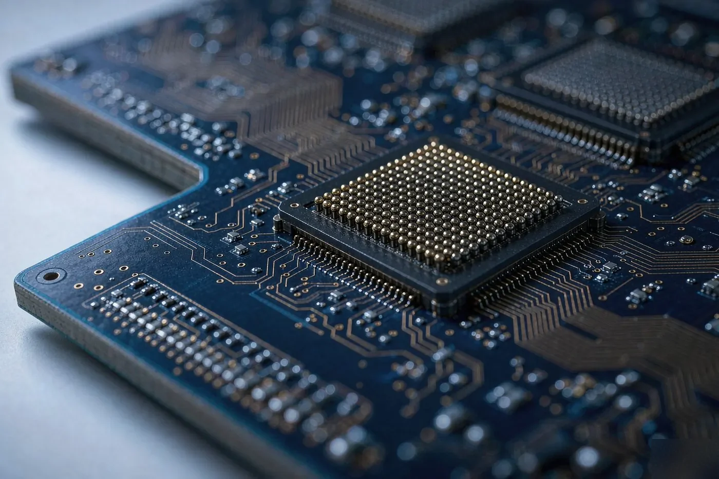
Rigid multilayer, HDI, heavy copper, metal-core and ceramic substrates. 1–44 layers, 2/2 mil trace and space, 610 × 1100 mm maximum panel, up to 25:1 aspect ratio.
PCBA Assembly
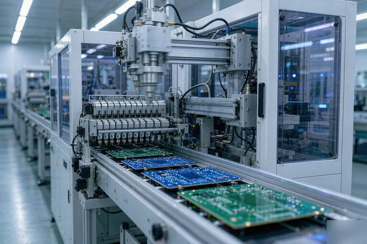
SMT, through-hole, BGA and QFN placement, turnkey component sourcing, ICT/FCT functional test and box build. Four SMT lines at 500k placement points per day, on the same campus as fabrication.
Substrate Selection
FR-4 Tg classes, halogen-free, metal-core, polyimide flex and low-loss RF laminates — compared on Dk, Df, thermal rating and cost, with a stocked-grade list and a selection guide.
The numbers we quote against
These are the figures published on the capabilities page, which is the authoritative source for every specification on this site.
Every board earns its certificate on data
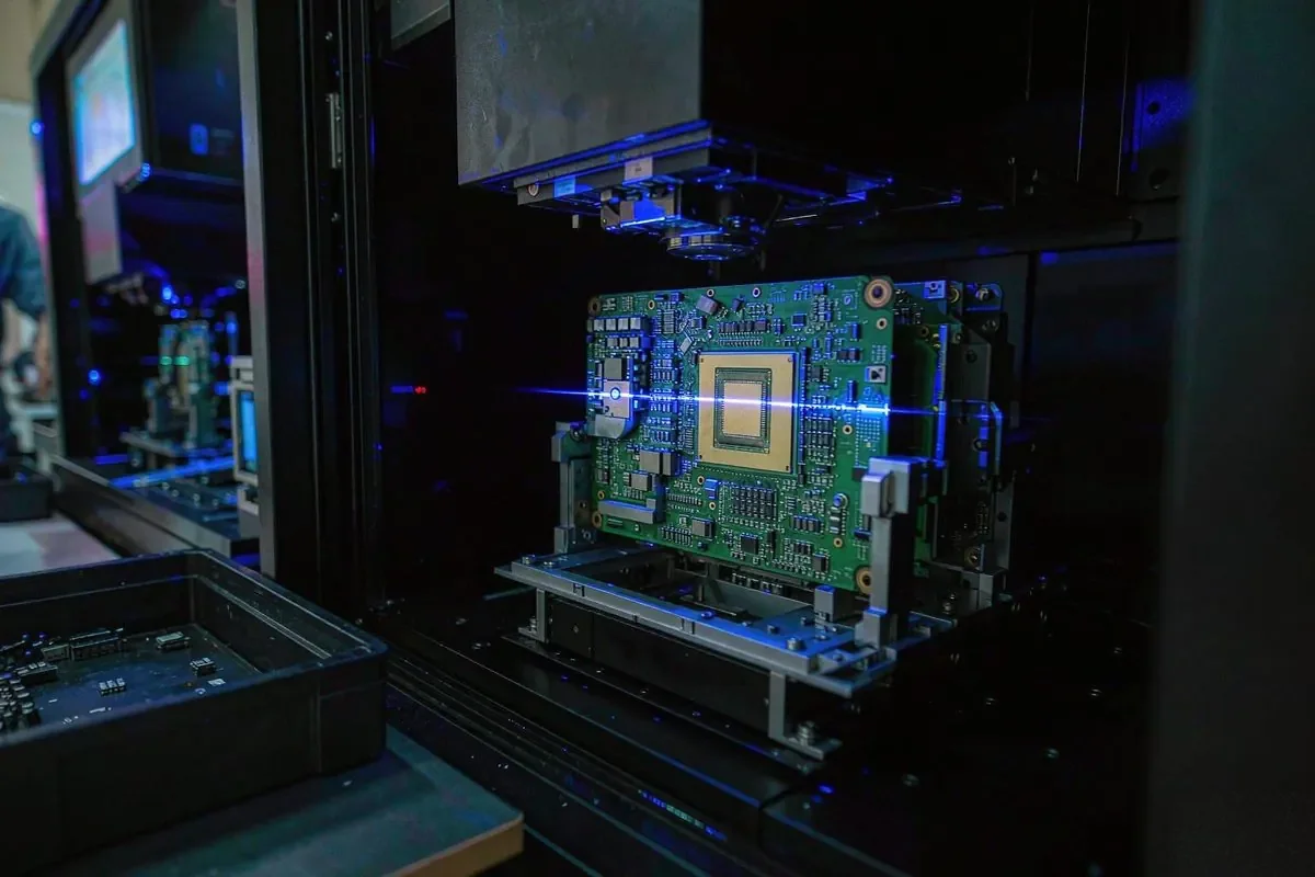
Flying-probe and fixture test, SPI before placement, AOI after etch and after assembly, X-ray on BGA and via-in-pad. The pass rates behind these numbers are published — not claimed — on our quality page, updated with real production data.
- 99.8% first-pass yield, 99.5% mass-production yield
- Impedance coupons tested on every controlled-impedance order
- Full traceability from laminate batch to shipment
Built for the markets we ship into
Different industries fail boards for different reasons. Here is what each one usually pulls from our capability set.
AI & Data Centre
High-layer-count server and accelerator boards with dense BGA fields and controlled-impedance serial channels.
Telecom & RF
Baseband, antenna and microwave front ends where loss tangent and Dk stability decide the design.
Automotive
Thermal-cycling-rated boards assembled under IATF 16949 discipline, with full traceability.
Medical
Diagnostic and wearable electronics requiring consistent inspection records and halogen-free material options.
Industrial & Power
Motor drives, converters and controls carrying real current on boards that must survive the factory floor for a decade.
Consumer Electronics
Cost-optimised builds where panelisation arithmetic and standard materials decide the margin.
Answer the stackup question first
Most quote delays come from a specification that has not been pinned down yet. These calculators let you settle impedance, stackup symmetry, copper current and unit conversion before you send anything.
Impedance Calculator
Microstrip, stripline and differential pair impedance from your own stackup geometry and dielectric constant.
Stackup Designer
Build a symmetric multilayer stackup, check copper balance, and export the layer table to attach to your RFQ.
Copper Current Calculator
Required trace width for a target current and temperature rise, based on IPC-2221 curves and copper weight.
PCB Unit Converter
mil, mm, µm, oz, AWG — convert between the units that actually appear on PCB drawings and stackup tables.
Written to be quoted
Original English material from our process engineers. Every page states the governing standard, the numbers involved, and where the practical limit actually is.
Start from first principles
How a board is actually built, layer by layer, and which choices are locked in at which stage.
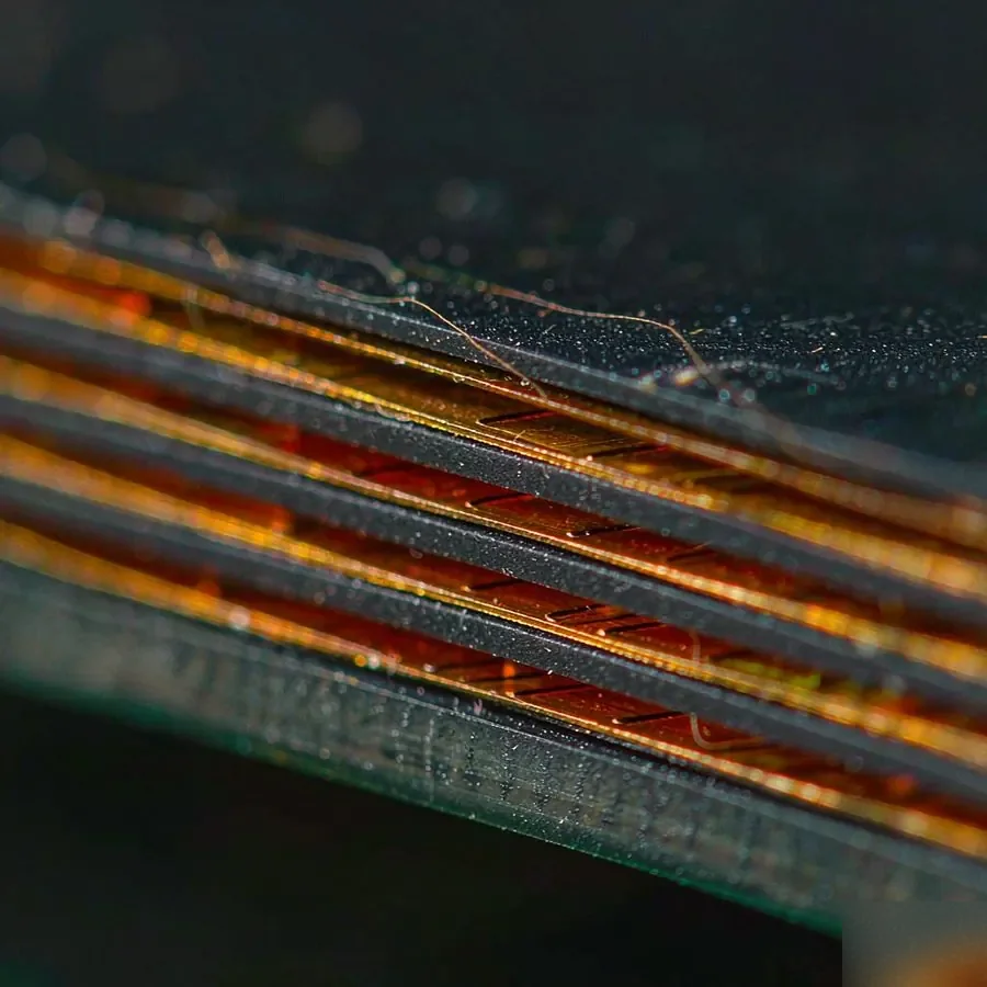
- How a multilayer PCB is laminated
- Plated through, blind, buried and micro-vias
- Solder mask, silkscreen and surface finish
- What DFM review actually checks
Pick the substrate on data
Dielectric constant, loss tangent, thermal rating and cost, compared across the grades we actually stock.
- FR-4 vs high-Tg vs halogen-free
- Rogers, Taconic, Panasonic M6/M7, TUC
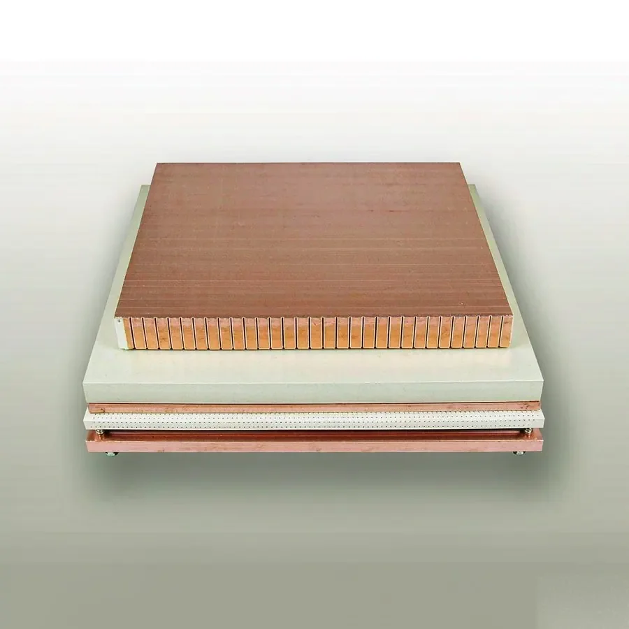
- Aluminium and copper metal-core
- Al₂O₃ and AlN ceramic substrates
Where the limits come from
Why a 25:1 aspect ratio changes plating time, why ±8% impedance needs a coupon, and what drives heavy-copper pricing.
- Drill aspect ratio and plating uniformity
- Impedance control and test coupons
- Heavy copper etching and fill
- Panelisation and material utilisation
Three sites, three jobs
Lingxin runs three sites deliberately, so that nobody has to read past content they do not need. Here is which one fits your enquiry.
Go to aipcb.cc
Our high-end line handles the layer counts, HDI stacks and RF materials that need a dedicated process window. Technical write-ups are in Chinese.
aipcb.cc →Go to ipcba.com.cn
Component sourcing, SMT and through-hole assembly, functional test and final packaging, quoted as one delivered unit. Content in Chinese.
ipcba.com.cn →You are already here
ipcb.cc carries the group's English content and the calculators. Quote in English, specifications in English, answers in English.
Start a quote →Questions we get before the first drawing
What is ipcb.cc?
What is the minimum and maximum layer count?
Can I get an instant price online?
What is your minimum trace and space?
0.05 mm) for standard multilayer work. Trace width accuracy is ±8 µm and controlled impedance tolerance is ±8%.Which certifications do you hold?
Do you manufacture outside China?
Start Your PCB Project
Send your Gerber files, stackup requirements and quantity. An engineer reviews every enquiry and replies within 24 hours — not a sales auto-reply.