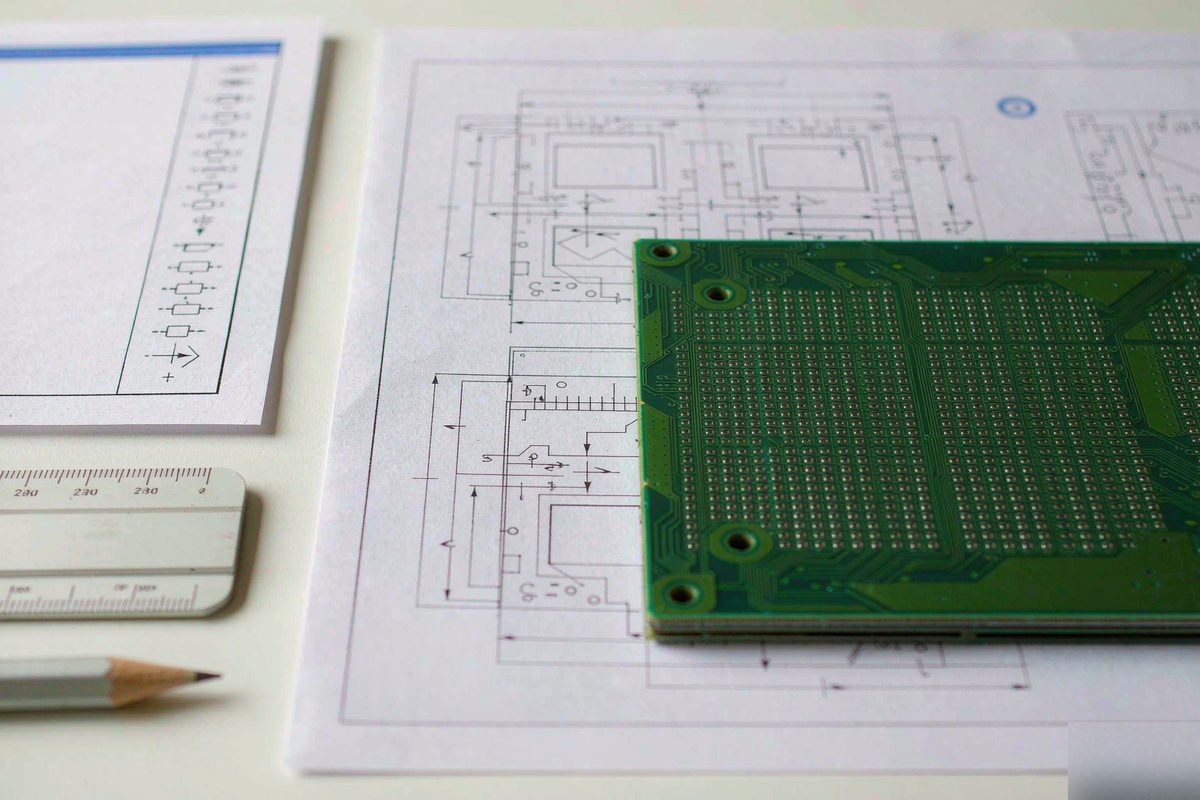
PCB 101 — how a board is actually made
A printed circuit board starts as a sheet of copper-clad laminate and ends as a tested interconnect.
Between those two points the board is drilled, plated, imaged, etched, laminated, masked and finished,
and each of those stages has a tolerance that constrains what you can design. Most manufacturability
questions are decided in the first three stages, long before anyone looks at a solder mask colour.
Inner layers first. On a multilayer board the inner copper layers are imaged and
etched before anything is laminated, so their line width and spacing are set at that point and cannot be
recovered later. Registration — whether layer 3's features land on top of layer 5's — then
depends on how accurately the stack is aligned during lamination and how much the prepreg moves as it
cures. Above eight layers we use X-ray drill targeting after lamination specifically because mechanical
registration alone is no longer good enough.
The drill determines the plating. A via is a hole with copper plated through it, and the
plating has to reach the middle of the hole. The ratio of board thickness to drill diameter — the
aspect ratio — governs how hard that is: at 8:1 it is routine, at 20:1 the plating solution
circulates poorly and the barrel thins in the centre, and at 25:1 the process needs to be run
deliberately slowly and checked by cross-section. This is why a 3.2 mm board with 0.2 mm vias costs
materially more than a 1.6 mm board with the same vias.
Etch tolerance is the hidden variable. Etching removes copper sideways as well as
downwards. On 1 oz copper this undercut is small; on 6 oz it is not, which is why heavy-copper boards
need either a wider nominal trace or a stepped etch to hold the width. The number we publish,
±8 µm trace width accuracy, is the figure that holds across our standard
process window — it is not a guarantee on an arbitrary 13 oz inner layer.
Substrate materials
Pick the material on dielectric constant, loss tangent, thermal
rating and cost — in that order of what actually constrains the design.
| Material | Dk | Key property | Use it when |
|---|
| Standard FR-4 | 4.2–4.5 | Tg 130–140 °C, lowest cost | General multilayer, consumer, leaded assembly |
| High-Tg FR-4 | 4.2–4.6 | Tg 170–180 °C | Lead-free reflow, thermal cycling, thicker boards |
| Halogen-free | 4.3–4.7 | IEC 61249-2-21 compliant | Regulated markets, EU electronics |
| Rogers RO4000 series | 3.3–3.6 | Low loss, stable Dk over temperature | RF, antenna, anything above 1 GHz |
| Taconic | 2.5–3.5 | Very low loss | Microwave, high-Q filters |
| Panasonic M6 / M7 | 3.3–3.6 | Low loss, good CTE match | High-speed digital, 25 – 56 Gbps channels |
| Polyimide | 3.4–3.8 | Flexible, high temperature | FPC, rigid-flex, high-temp cycles |
| Aluminium core | — | 2–12 W/m·K | LED lighting, motor drivers, cheap thermal relief |
| Copper core | — | 2–12 W/m·K, high current | Power modules where the board carries the current |
| Al₂O₃ / AlN ceramic | 9–10 / 8–9 | Up to 170 W/m·K | High-power RF, power modules, no organic outgassing allowed |
Process explainers
Why does an aspect ratio limit exist at all?
Plating is an electrochemical process: copper ions have to reach the middle of the
hole and be reduced onto the barrel wall. In a deep, narrow hole the solution exchanges slowly, so
the deposited copper thins in the centre — sometimes to the point of a void that passes a
continuity test at room temperature and fails after thermal cycling. Our standard window is 8:1,
we run up to 20:1 routinely, and backplanes up to 25:1 with process controls and cross-sectioning.
Beyond that, the honest answer is that the design should be split or the vias should be larger.
What does ±8% impedance tolerance actually mean?
The impedance of a finished trace depends on five things: trace width, dielectric
height, copper thickness, dielectric constant and the presence of nearby copper. All five vary in
production. ±8% is the window we hold when a board is specified as impedance-controlled and
we build and measure a coupon on the panel. It is not a statement about any unmeasured trace, and it
is not a statement that a board without coupons is ±8%. If impedance is critical, specify
coupons — the report ships with the boards.
Why is heavy copper so much more expensive?
Three reasons. Etching 6 oz copper without undercutting needs a slower etch and a
wider nominal trace. Thick copper does not fill fine features well, so inner layers often need
copper fill or a stepped etch to keep the dielectric thickness in range, which adds process steps.
And a board carrying 10 oz copper is physically stiffer, so everything from lamination pressure to
routing changes. The price difference is process, not margin.
When is panelisation a design decision rather than a manufacturing one?
More often than most designers expect. Panel utilisation determines how much
laminate is consumed per board, and on a small board that can move unit price by 20–30%.
Rotating a design 90°, allowing a shared tooling strip, or accepting a slightly different
outline can all change the price without changing the board. If a design is cost-sensitive, send
the outline early and ask what the best panelisation would be — before the layout is frozen.
Does a DFM review change the price or the schedule?
It does not change the price — DFM review is included on every order. It can
change the schedule, because a review that finds a real problem adds a day while you decide. A
review that finds nothing costs you nothing. That asymmetry is deliberate: it is much cheaper to
change a Gerber file than to scrap a panel.
Engineering guide · Surface finish
Surface finish selection without the folklore
Every finish is a compromise between solderability, flatness, shelf life, wire-bondability and
price. There is no "best" one — there is the one that matches your assembly process,
component pitch and shelf logistics. Here is how we talk customers through it:
ENIG — the default for fine pitch
Flat, corrosion-resistant, works for BGA and 0.3 mm-pitch QFP, stores for a year. It costs
more than HASL and has one known failure mode: black pad, where the nickel corrodes
before gold plating and the joint later cracks. We control it with bath chemistry monitoring
and a phosphorus-content check; if your board is high-reliability, ask for the coupon report.
HASL — still the cheapest good option
Lead-free HASL is durable, reworkable and forgiving. Its weakness is flatness: the meniscus
leaves domed pads that are wrong for 0.4 mm-pitch parts and for any press-fit pin. For
through-hole and coarse-pitch work, it remains the value choice.
OSP — flat, cheap, and on a clock
OSP is the flattest and cheapest finish, with two constraints: a shelf life measured in months,
and it survives limited reflow passes. Perfect for high-volume single-side SMT runs that ship
straight to your line; wrong for boards that sit in a drawer.
Immersion silver and immersion tin
Silver solders beautifully and stays flat, and is friendlier to high-frequency skin effect than
nickel-bearing finishes — the trade is tarnish management in packaging. Tin is flat and
press-fit friendly; watch for whisker risk on pure-tin systems in fine-pitch, long-shelf-life
applications.
Hard gold and ENEPIG — specialist tools
Hard gold over nickel belongs on edge connectors and keypads, where contact resistance and
insertion cycles dominate. ENEPIG adds palladium and solves black pad while staying
wire-bondable — the premium answer for gold-wire assemblies. Neither is a general-purpose
finish; both price accordingly.
Quick pick: BGA or <0.5 mm pitch → ENIG. Coarse pitch,
cost-driven → lead-free HASL. High-volume SMT, fast consumption → OSP. RF front end
→ immersion silver. Edge connector → hard gold. Gold-wire bonding → ENEPIG.
Engineering guide · DFM
The DFM checklist we run before your board is built
DFM review is included on every order, and it is not a formality — it is a fixed checklist
of the failure modes that actually scrap panels. This is the list, so you can pre-check before
sending Gerbers:
- Annular ring against layer count and drill tolerance — the single most
common first-article rejection.
- Trace/space vs copper weight — 2/2 mil is a 1 oz figure; etch
undercut widens the rule on 3 oz and above.
- Aspect ratio — board thickness divided by the smallest drill; 8:1
standard, 20:1 with process controls, 25:1 backplane-class.
- Copper-to-edge clearance — 0.30 mm minimum unless edge plating is
specified.
- Thermal relief spokes on plane connections to vias and pads — solid
connections on big planes make hand soldering impossible and reflow profiles unreliable.
- Solder mask dams between fine-pitch pads — below a certain pitch the
dam cannot be held and the pads must be mask-free by design.
- Silkscreen over pads and vias — the classic self-inflicted assembly
defect; we check it even when the fab drawing does not.
- Panelisation and depaneling — tab-route vs V-score vs edge rail; width,
fiducials, and whether a 5-axis router or a V-scoring line depanels it.
- Impedance reference planes — every controlled trace needs an unbroken
reference beneath it; we check the plane splits before quoting tolerance.
- Via-in-pad — flagged for fill-and-cap unless tented vias are explicitly
acceptable under the part.
- Paste layer vs footprint — aperture ratio and home-plate adjustments for
reflow yield, checked at assembly handoff.
- Balanced copper distribution across the panel — asymmetric copper warps
boards in reflow; we may add thieving or ask for a stackup change.
What DFM costs you: nothing if it passes, a day if it flags a real problem.
What skipping it costs: a scrapped panel and a slipped schedule. The asymmetry is the whole point.
Engineering guide · Cost
Paying less for the same board
Board price is dominated by laminate consumption and process steps, not by layer count alone.
Three levers move it more than most buyers expect:
- Panel utilisation. A 105 × 85 mm board on our 610 × 1100 mm
panel wastes less material than a 110 × 90 mm one, because the panel arithmetic
changes. On small boards this alone can move unit price by 20–30%. Send the outline early.
- Standardise what does not matter. Green mask ships fastest; exotic thicknesses
and non-stocked copper weights add process steps. Every "special" that survives into the spec
should have a reason.
- Quantity breaks are real but not linear. The unit price curve drops steeply
from 1 to 100 pieces, then flattens. If 60 pieces covers the year, ordering 60 beats ordering
30 twice — one setup charge, one tooling charge, one shipment.
Try the instant quote with different quantities and
sizes — the cost breakdown shows each factor's contribution, so the trade-offs are visible
before you commit a layout.